Description
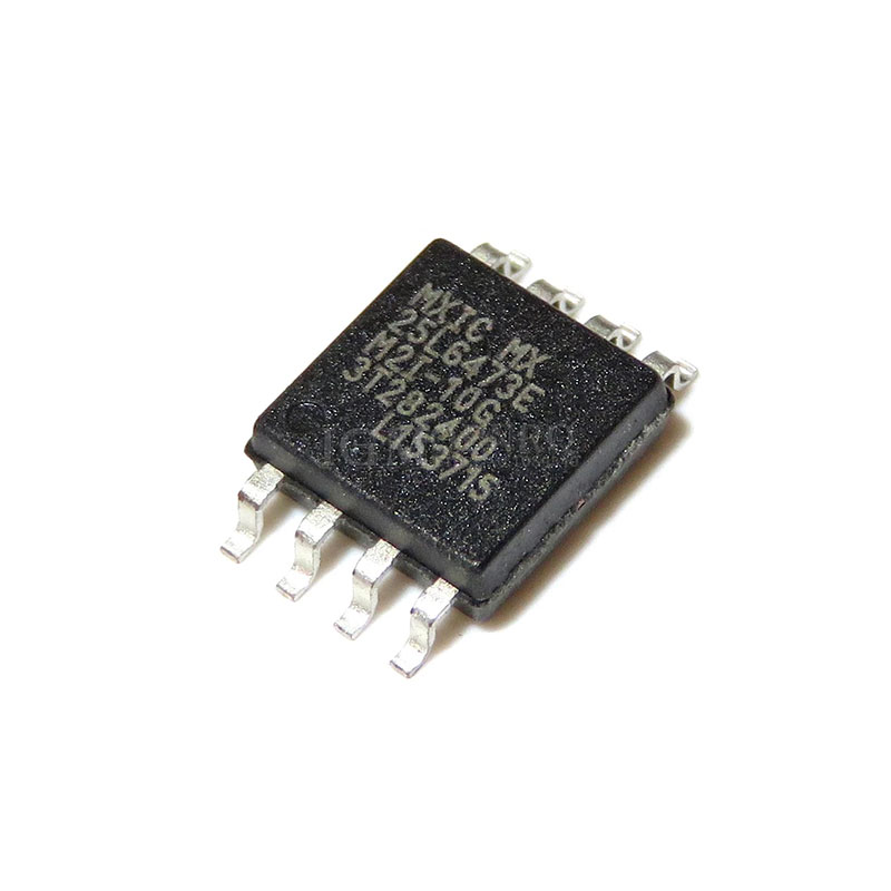
MX25L6473E is 64Mb bits Serial Flash memory, which is configured as 8,388,608 x 8 internally. When it is in two or four I/O mode, the structure becomes 33,554,432 bits x 2 or 16,777,216 bits x 4.
MX25L6473E features a serial peripheral interface and software protocol allowing operation on a simple 3-wire bus while it is in single I/O mode. The three bus signals are a clock input (SCLK), a serial data input (SI), and a serial data output (SO). Serial access to the device is enabled by CS# input.
MX25L6473E, MXSMIO® (Serial Multi I/O) flash memory, provides sequential read operation on the whole chip and multi-I/O features.
When it is in dual or quad I/O read mode, the SI pin and SO pin become SIO0 pin and SIO1 pin for address/ dummy bits input and data output.
After the program/erase command is issued, auto program/erase algorithms that program/erase and verify the
specified page or sector/block locations will be executed. Program command is executed on a byte basis, or page (256 bytes) basis, or word basis for Continuous Program mode, and erase command is executed on 4K-byte sector, 32K-bytes/64K-byte block, or whole chip basis.
To provide the user with ease of interface, a status register is included to indicate the status of the chip. The status read command can be issued to detect the completion status of a program or erase the operation via the WIP bit.
When the device is not in operation and CS# is high, it is put in standby mode.
The MX25L6473E utilizes Macronix’s proprietary memory cell, which reliably stores memory contents even after 100,000 program and erase cycles.


